| |
Base
8 Digits
|
|
| |
Purpose:
To display the values from ' 0 ' to ' 7 ' in the
seven segment display unit of the development board
using the MACH 4 - 64/32 CPLD.
Procedure:
Double
click on the ISP Design Expert icon. The ISP Design
Expert window will appear. This is how it looks like:
|
|
| |
|
|
| |
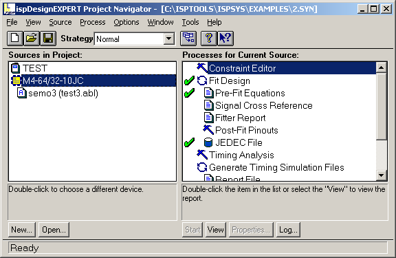
Click
on the 'File' tab and select ' New project '. When prompted
to save the newly created project, I saved it as "2.syn".
We can change the Name of the project by double clicking
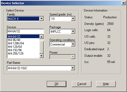
the upper icon in the sources box. The default device
is (ispLSI5384VA-125LB388). We change the type of device
by double clicking on the yellow CPLD icon: |
|
| |
 |
|
| |
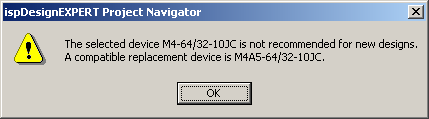
If
you get some messages like this choose OK and then confirm
the change by choosing "Yes":
|
|
| |
 |
|
| |
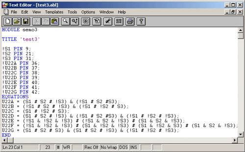
We
add a new source by choosing 'Source' and then 'New...'
and then 'ABEL HDL Module'. I chose the module name
"semo3" and the title "test3". Then
choose OK. We see that there is some automatic code
generated. This is how the Text Editor looks like:
|
|
| |
 |
|
| |
You
can see the program in the capture above or you can
download it from here: test3.abl.
There is more detailed information about the making
of the program in "The Program" section
|
|
| |
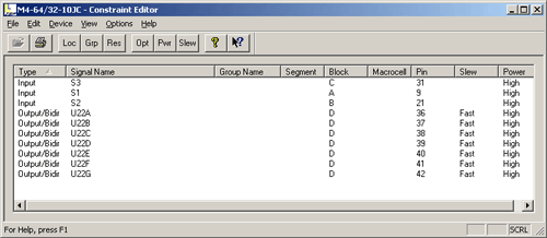
Select
the device (M4-64/32-15JC) from the left pane and double
click the 'Constraint Editor' on the Right pane. Once
the constraint editor has initialized, select ' LOC
' from the toolbar to assign the correct PIN numbers
to the switches and segments ( the box next to the Output
must be checked in order to get the full list of the
segments). Use the " pin out of the CPLD (both
MACH4-32/32 and MACH4-64/32) on the development board
" datasheet from the Digital Systems Lab web server
for the correct pin assignments.
!REMARK: when assigning the pins use the leftmost
column of the table to get the correct pin numbers.
DO NOT use the second one. The first time when I did
the program I made the wrong associations and got compilation
errors.
|
|
| |
 |
|
| |
The
image above represents the Pin assignments window. Once
all the pins and switches have been assigned, minimize
the constraint editor, plug in the JTAG download cable
into the parallel port of the laptop, connect the power
supply to the development board and run ' Fit Design
' (found on the right navigator window of the ispDesignExpert)
by double clicking on it. Once the ' Fit Design ' has
completed, a JEDEC file by the name of ' 2.jed ' was
created in the same directory as the "test3.abl'.
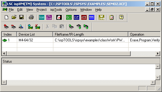
The next step involves downloading the design on to
the M4-64/32 CPLD on the development board. In order
to do this, run the ' ispVM System '. With the power
supply connected to the development board and the
JTAG download cable connected to the laptop, click
on ' Scan ' in the toolbar to automatically detect
the CPLD on the development board. Once the M4-64/32
appears on the device list, double click on it to
get the device information dialog box. The image below
is a capture from the ispVM System:
|
|
| |
 |
|
| |
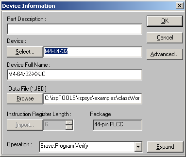
You
can change the description for the device manually and
change the path for the .jed file:
|
|
| |
 |
|
| |
After
specifying the JED file click on OK, click on the '
Go ' in the toolbar to begin the download. Once the
download is completed you see the "0" digit
and you are ready to test the system.
|
|
| |
The
Program:
First of all assign switch combinations to the numbers
0 through 7 inclusive.
(! = NOT; & = AND; # = OR)
0 = ! Sw1 & ! Sw2 & ! Sw3
1 = Sw3
2 = Sw2
3 = Sw2 & Sw3
4 = Sw1
5 = Sw1 & Sw3
6 = Sw1 & Sw2
7 = Sw1 & Sw2 & Sw3
Once the switches have been assigned create the truth
table. The SSD (seven segment device) appears as shown
below.
|
|
| |
 |
|
| |
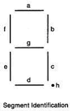
The
segments are represented by the letters from ' a ' to
' g ' inclusive. Hence to obtain a 0 all the segments
except ' g 'would have to be in the active state (i.e.
lit up). Similarly, to get a 1 only ' b ' and ' c '
would have to be in the active state. The same procedure
applies to all the other numbers. The truth table for
the numbers is shown below:
| |
|
|
| |
|
Sw1
|
Sw2
|
Sw3
|
|
a
|
b
|
c
|
d
|
e
|
f
|
g
|
|
0
|
0
|
0
|
|
1
|
1
|
1
|
1
|
1
|
1
|
0
|
|
0
|
0
|
1
|
|
0
|
1
|
1
|
0
|
0
|
0
|
0
|
|
0
|
1
|
0
|
|
1
|
1
|
0
|
1
|
1
|
0
|
1
|
|
0
|
1
|
1
|
|
1
|
1
|
1
|
1
|
0
|
0
|
1
|
|
1
|
0
|
0
|
|
0
|
1
|
1
|
0
|
0
|
1
|
1
|
|
1
|
0
|
1
|
|
1
|
0
|
1
|
1
|
0
|
1
|
1
|
|
1
|
1
|
0
|
|
1
|
0
|
1
|
1
|
1
|
1
|
1
|
|
1
|
1
|
1
|
|
1
|
1
|
1
|
0
|
0
|
0
|
0
|
|
|
| |
|
|
The
equations for each of the segments are evaluated by
taking relevant the CNF (Conjunctive Normal Form - Product
of Sums (for all output = 0)) or DNF (Disjunctive Normal
Form - Sum of Products (for all output = 1)). So, taking
DNFs and CNFs, we have :
a
= (Sw1 # Sw2 # ! Sw3) & (! Sw1 # Sw2 # Sw3);
b = (! Sw1 # Sw2 # ! Sw3) & (! Sw1 # ! Sw2 # Sw3);
c = (Sw1 # ! Sw2 # Sw3);
d = (Sw1 # Sw2 # ! Sw3) & (! Sw1 # Sw2 # Sw3) &
(! Sw1 # ! Sw2 # ! Sw3);
e = (! Sw1 & ! Sw2 & ! Sw3) # (! Sw1 & Sw2
& ! Sw3) # (Sw1 & Sw2 & ! Sw3);
f = (! Sw1 & ! Sw2 &!Sw3) # (Sw1&!Sw2&!Sw3)#(Sw1&!Sw2&Sw3)#(Sw1
& Sw2 & ! Sw3);
g = (Sw1 # Sw2 # Sw3) & (Sw1 # Sw2 # ! Sw3) &
(! Sw1 # ! Sw2 # ! Sw3);
|
|
| |
Observations:
-At the beginning the "0" digit is on
-if we press sw3 =>1, sw2=>2, sw2&sw2=>3,
sw1=>4, sw1&sw3=>5, sw1 & sw2=>6,
sw1&sw2&sw3 =>7
|
|
| |
Problems
and Conclusion:
Again the common error that the pins and segment are
actually ' active low ' and not ' active high
'. You can correct this problem by simply negating (!)
the switches and segments in the PIN description part
of the program.
I also did bad pin associations because I did not use
the first column of the pin sheet. (see the remark).
There were also some minor problems related to syntax
or bad hardware configuration but this always happens
when you are a beginner.
|
|
| |
Modifications
to the program:
We
can also derive a program that displays the numbers
according to their two's complement representation,
the most significant bit (SW1) is used as a sign bit:
| SW
1 |
SW2 |
SW3 |
SSD
Number |
| 0 |
0 |
0 |
0 |
| 0 |
0 |
1 |
1 |
| 0 |
1 |
0 |
2 |
| 0 |
1 |
1 |
3 |
| 1 |
0 |
0 |
(-)
4 |
| 1 |
0 |
1 |
(-)
3 |
| 1 |
1 |
0 |
(-)
2 |
| 1 |
1 |
1 |
(-)
1 |
We
change the boolean expressions and use an extra SSD
LED for the sign. This is the program:
module
TCom
!sw1
                          pin;

                          !sw2 pin;

                          !sw3 pin;

                          !u22a pin;

                          !u22b pin;

                          !u22c pin;

                          !u22d pin;

                          !u22e pin;

                          !u22f pin;

                          !u22g pin;

                          !u26g pin; "used for minus sign
equations
u22a
                          = (sw1#sw2#!sw3)&(!sw1#sw2#sw3)&(!sw1#!sw2#!sw3);

                          u22b = 1;

                          u22c = (sw1#!sw2#sw3)&(!sw1#!sw2#sw3);

                          u22d = (sw1#sw2#!sw3)&(!sw1#sw2#sw3)&(!sw1#!sw2#!sw3);

                          u22e = (!sw1&!sw2&!sw3)#(!sw1&sw2&!sw3)#(sw1&sw2&!sw3);

                          u22f = (!sw1&!sw2&!sw3)#(sw1&!sw2&!sw3);

                          u22g = (sw1#sw2#sw3)&(sw1#sw2#!sw3)&(!sw1#!sw2#!sw3);

                          u26g = sw1;
end
|
|
| |
| The
movie of the experiment -this is the .avi
demonstration of how the program works. |
|
|